Tag Archives: stm32

STM32G4 ADC performance part 2

Back last year, I walked through bisecting and debugging an annoying problem that caused the STM32G4 ADC on the moteus controller to exhibit higher than expected noise in result largely to either the exact placement in flash of the initialization code, or to the exact timing of the initialization. While the immediate glaring sharp edge was removed, the resulting performance still was confusing to me, and looked like it was not yet optimal. Further, a moderate percentage (2% or so), of production boards failed end-of-line tests related to the current sense noise in ways that were hard to fix by swapping components. Because of this, I wanted to dive in and investigate further. This is that process.

Tips and theories from the interwebs

In response to the original article, I received a *wide* variety of tips, leads, theories, and proclamations, some of which were more credible than others. Here are the top categories:

  • Incorrect clock or prescaler configuration
  • Some sort of clock domain synchronization problem causing prescaler configuration to be incorrectly set
  • Insufficient VREF+ decoupling
  • ADC initialization phasing

Some of these could be easily ruled out using just the information in the original article. Notably that the prescaler was documented to have been set to a frequency that was well within the range of what the ADC was capable of and that it was also read back from the peripheral and shown to have the correct value later in time.

That rules out the first two issues. To tackle the rest, I first needed to build some tools.

Quantifying the problem

Before attempting to confirm or refute the remaining hypotheses, I wanted to be able to better quantify the problem. In that vein, I made some tools and scripts which would attempt to render what noise was present as a function of reported ADC counts. The idea was to sweep each phase of the motor through a range of fixed voltages, and capture a time domain signal at a variety of steady state points. Then, we would plot the magnitude of the noise, and what the the frequency components looked like throughout the range.

The resulting tool set consists of a set of scripts to perform the sampling and then an interactive matplotlib based tool to render the results. It looks like this:

The top 3 plots in the top window show log-normalized spectrograms at each ADC count for each channel. The line graph in the top window shows the overall standard deviation of each channel at each ADC count. The bottom window shows the time domain signal at any given point — clicking on any of the top channels will switch to that given time domain plot. This lets you explore many possible hypotheses, especially those that are not necessarily best represented as noise in the frequency domain. Since the sweeps are over fixed voltages on each channel, the range of ADC values sampled are not the same for each channel, as the zero point bias is different for each channel and board. The big “X”s on the standard deviation plot shows where the zero point was for each channel.

In this particular plot (which is from a random intermediate test), you can see that there are definitely some frequencies which have noise that is periodic at every 8 LSB interval, channels 1 and 2 have significant wide-band noise from around 2030 to 2048, and channel 0 has an additional high frequency noise component from around 2041 to 2048.

Cycle accurate phasing

The next piece of infrastructure I needed to investigate this was to be able to make cycle accurate delays on the STM32G4, and have a delay end at a specific value of the global cycle counter. This is actually relatively hard, as there exists a flash accelerator, instruction cache, and data cache which all work to make accurate timing difficult, yet cannot be permanently disabled or things run too slowly. This is combined with the fact that when operating under the debugger, peripherals like the cycle counter are unreliable.

My solution was to first run the delay completely from the STM32G4’s CCM SRAM (which the ISR in moteus already was using). This takes the flash accelerator out of consideration. Next, the instruction and data caches are manually flushed before entering the critical section. Finally, the entire routine is implemented in assembly, with a superstitious number of alignment directives thrown in for good measure.

To calibrate the offset constants, I carefully set a breakpoint only on the first instruction after the sequence, and ensured that the CPU’s cycle counter was equal to the intended calculated one at every instance across a few different shufflings of code and compilations.

At this point, I could cause each ADC to be initialized at a specific CPU cycle counter value (or really any other operation), in a repeatable manner.

Preemptive solution: VREF+ decoupling

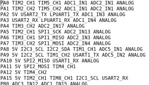
The ADC in the STM32G4 series operates on a successive approximation principal using switched capacitors. With that technique, at each clock cycle, various capacitors are either switched to VREF+ or to ground in order to more closely approximate the captured input voltage. Thus large current transients on VREF+ can occur, especially when the higher order bits in the sample are altered. These large transients, coupled through higher than desired impedance in the VREF+ signal path, can the VREF+ voltage to sag, resulting in faulty comparisons. The low-pin count STM32G4 variant that moteus uses is even more susceptible to this phenomenom as it has no dedicated analog ground pin. For the UQFN48 package, all grounds are tied to the exposed pad under the chip.

This particular failure mode is most likely to occur at voltages just below the halfway point, so below 2048 for the 12 bit STM32G4 ADC. If the first comparison is performed with a sagging VREF, and the actual voltage should have been, say 2044, it may erroneously be placed in the >= 2048 bucket, and then all subsequent comparisons will report it to be smaller thus resulting in exactly 2048 being the final result.

Even before attempting diagnosis, I went ahead and improved the situation for the moteus-n1, as it was in the design process anyway. The moteus r4.11 VREF+ decoupling did meet the official datasheet constraints of a 1uF ceramic capacitor close to the chip, but the ground path for that capacitor may not have been optimal, and 1uF may be insufficient for 5 simultaneous ADC operations. For the moteus-n1 r1.3 board, both a larger 4.7uF capacitor was used for the bulk, along with a separate smaller, 0.1uF capacitor. Also, additional ground vias were placed under the exposed pad along the entire side of VREF+, so that the full current path is short. Here is the resulting layout:

Here, pin 20 is VREF+, C10 is the primary 4.7uF decoupling capacitor, and C87 is the smaller capacitor. The ground path for the large capacitor is basically as short as physically possible, and 4 vias connect the ground plane to the STM32G4 all along that side.

Experimental flailing

Given these tools, I was able to make some progress.

First, I ran the before and after on the fix from the original post:

Problematic on left, “improved” on right

The fix definitely made things better, in that channel 0 and 2 had only a small non-linearity around 2048, although channel 1 still had a drastic deviation around 2048.

From looking at this, and fiddling with things, it seemed that with the moteus ADC configuration, the ADCs were definitely sensitive both to the exact cycle count phasing between their initialization, and the exact cycle phasing between any ADC and some system level phenomena. After a lot of fiddling around with the above tools, I hit upon the idea of sweeping through different possible options of inter-ADC cycle timing and from-boot cycle timing.

Note, for the purposes of the results below, the moteus controller was configured with a 170MHz AHB clock, a 2x divider to the APB1/APB2 clocks, the ADCs were configured to run asynchronously, their clock source was the peripheral clock, and the ADCs had an 8x prescaler.

Here are some example plots showing a few of the sample permutations:

8 LSB periodic noise that various with the CPU cycle modulo 2

In this instance, ADC3/4 were initialized with a 4 CPU cycle offset from ADC1/2

No matter the spacing between ADC initializations, the results of all ADCs were materially better or worse depending upon when the first was enabled on a 2 CPU clock cycle boundary. I did not have a repeatable reference from power-on for the system, so it was arbitrary which was good or bad, but in any given firmware image it would look like:

  • first adc enable at CPU cycle offset 0: good
  • first adc enable at CPU cycle offset 1: bad
  • first adc enable at CPU cycle offset 2: good
  • first adc enable at CPU cycle offset 3: bad

Similarly, no matter what the state of the system from the first ADC enable phase, things could get worse if the individual ADCs were started in different phases relative to each other. This relationship was more complicated, but roughly followed a 16 CPU clock cycle. Results were best when the CPU cycle counts between when the ADCs were enabled was an even 16 cycles and was various degrees of worse at different phasings.

The “actual” problem

After figuring out the above, I was close to a fix. I could easily control the spacing between ADC initializations, but had not discovered a way to control the phasing between the first ADC initialization and whatever system level phenomena led the to the 2x period (likely due to the 2x AHB/APBx divider). It was at this point that I decided to go looking through the ST errata for the STM32G474 another time to see if I had missed anything.

And lo, while I hadn’t missed anything before, a new errata had been added in March 2023 which pointed to a more systematic resolution!

The errata gives three possible resolutions:

1: Do not execute ADC conversions concurrently. This is both not feasible in moteus, and in my experiments it does not completely resolve problems anyways.

2: Use the same clock for all ADCs AND an ADC prescaler of 1x. This is also not feasible for moteus, as a prescaler of 1x would have the ADC running much faster than the maximum possible speed.

3: Use a synchronous clock, the same clock configuration for all ADCs, and trigger them all simultaneously from a hardware timer with a compatible prescaler. This seems like a pointer to the best option, and hints at explanations for the problems I had before.

This errata perfectly describes all the confounding symptoms I initially had, where inserting various NOPs or re-arranging the code would cause the ADCs to either work well or give terrible results. Initializing the ADCs back to back made it much more likely that poor phasing would result, where doing them separately gave a larger room for chance to intervene.

Resolution

With the above errata and my experiments above, I now had a concrete path to a fix. The problem which had been hardest for me to resolve was the ambiguity about which of the APB phases the ADCs were enabled in. Using synchronous clocking presumably ensures that it is always the same one, and hopefully that phase is the “good” one.

For the triggering aspect, I tested two approaches, each of which gave identical ADC performance in my experiments. First, I switched the moteus software triggering to use a hand-rolled assembly block which triggers all the ADCs in 3 consecutive CPU cycles. Second, I had the PWM timer trigger a second timer through the internal hardware matrix, which then triggered the ADCs through the internal triggering mechanism. For whatever reason, TIM5 is incapable of driving the ADCs directly, thus the indirection requirement. This triggering improvement combined with the synchronous timer configuration removed all cases of periodic 8 LSB noise and instances of extremely large count 2048 noise.

With those changes in place, the results, while not perfect, are much improved. I verified them by using a variation of the cycle accurate delays above to add various delay phases of 1-8 cycles into the pre-main execution and between each ADC initialization to verify that the results were just as good in all cases. Interestingly, across a range of boards the moteus-n1 r1.3 results are about as good as the r4.11 results, which indicates that the VREF+ decoupling improvements, while a good thing overall, were not a significant contributor to at least these problems.

Final results, r4.11 left, n1 right

The git change implementing this can be found here:

Future work

As should be obvious, all of the above results above have one channel with significantly higher count 2048 noise. Interestingly, which ADC and channel it is differs between the r4.11 and n1. On r4.11 the offender is ADC1/IN12 (PB1) while on n1 it is ADC2/IN3 (PA6). I don’t know if it is channel specific within the MCU, or some board level deficiency that manages to only impact one channel or what. It still occurs even if the ADCs conversions are performed sequentially rather than in parallel, which at least rules out ADC cross contamination.

For now though, I’m leaving that as “future work”! Send me your thoughts!

moteus external connector pin selection

moteus r4.11 has two external connectors, the ABS connector (AUX2) and the ENC/AUX1 connector. The ABS connector was designed initially just to have 2 I2C pins. The ENC connector just has the random pins that were used for the onboard encoder SPI plus one more. Thus the range of external accessories that can be connected is somewhat haphazard and not necessarily all that useful.

When working on a more ground up revision of the controller, I wanted to improve that situation to expose more connectivity options on still a relatively limited connector set. The idea was to use 2 connectors, one which has 5 I/O pins and the other with 4 I/O pins. The onboard encoder SPI would still be accessible on the larger connector to use for at least one external SPI encoder, but how much other functionality could be crammed into the remaining pins? To start, lets see what possible options there are in the current firmware and supported by the STM32G4 microcontroller that moteus uses:

  • SPI: The larger connector by definition would have a set of SPI lines, MISO, MOSI, and SCK (now sometimes termed CIPO/POCI and COPI/PICO).
  • I2C: I2C requires two lines, one for data and one for clock.
  • ADC: Sine/cosine encoders and general purpose ADC inputs require analog inputs.
  • Quadrature: Quadrature encoders require two signal lines.
  • UART: Asynchronous serial lines can be used for a variety of purposes.
  • 5V Tolerant: While the STM32G4 used in moteus is 3.3V native, it can be convenient to support 5V inputs.

To be useful in the moteus firmware, most of these capabilities need to be accessed through STM32 specific hardware. The one exception is quadrature inputs, for which the firmware can manage slow to moderate rates using interrupts alone, but high rates requires hardware decoding. Complicating this, the STM32G4 only provides access to specific hardware peripherals on specific pins through the alternate function map:

My challenge was to figure out which microcontroller pins to assign to the 9 (5 on AUX1, 4 on AUX2) ports which maximized the number of hardware peripherals that could be used on each connector. There are a few additional twists that make this process more challenging than one would expect.

Multiple STM32 pins per connector pin

It is possible to connect multiple STM32 pins to the same external connector pin. With this, the software for any given user requested configuration can leave the unused pin in a high impedance mode where they will largely not effect the output. There are some constraints with this though, caused by the STM32 architecture.

If a pin without analog functionality is connected to an analog signal, then it has a permanently connected schmitt trigger attached. This will cause undesired behavior and power consumption at certain analog voltage levels. Pins with analog functionality have an additional switch to disconnect this. Thus if a user visible pin is intended to have analog inputs, then all the STM32 pins must have analog functionality.

Similarly, if a connector pin is intended to be 5V tolerant, then every STM32 pin connected to it must also be 5V tolerant.

The analog input pins are sprinkled across the 5 different ADC converters present on the STM32G4. Ideally, the pins would not all use the same ADC, so that the sampling window could fit into the existing ADC sampling time of the main interrupt service routine.

Doing the search

I first attempted to conduct this search by hand, but found that I had a hard time wrapping my head around the possibilities, kept getting lost back-tracking and ultimately could not keep all the constraints in mind at once. So… I wrote a tool! I ended up making a brute-force python script that consumes a simple one-pin-per-line encoding of the capabilities, takes some optional constraints like pins or peripherals to not use, and finds all possible configurations which optimize a metric.

Portion of pinout definition

I used this in two separate phases. First I ran it in a mode on the 4 user-pin connector to find a configuration where all user pins were 5V tolerant. Then for the 5 user-pin connector, I excluded the pins and peripherals used on the 4 pin connector, and added the constraint that the non-SPI pins had to be 5V tolerant. The onboard magnetic encoder also connected to these SPI pins is not 5V tolerant, so there was no reason to aim for that here. On this second phase, there were bonus points in the metric for how many other peripherals could be crammed into these 5V tolerant pins, since they could be used even while using the onboard magnetic encoder.

The tool has a few separate classes for each of the constraints. Each evaluates a pin configuration or subset of pins, and returns whether that constraint has been met, is inconclusive, or is impossible to meet. Enumerating the possible sets of pins was slightly complicated because of the optional “pin doubling” that can occur. I ended up using an encoding of the problem that made this not too troubling.

Results

In the end, I met nearly all of my goals. The 4 pin connector looks like:

Connector PinSTM32G4 PinFunctions
1PF15V / SPI / ADC
2PA10 / PF05V / SPI / UART_RX / I2C_SDA / ADC
3PA11 / PC45V / SPI / UART_TX / I2C_SCL / ADC / QUAD_3A
4PB75V / UART_RX / QUAD_3B

The only real downsides here are that if hardware quadrature is used, then neither USART nor I2C can be used simultaneously.

For the 5 pin connector, the following assignment was chosen:

Connector PinSTM32G4 PinFunctions
1PA5 / PB14SPI / QUAD_1A / ADC
2PB4SPI / QUAD_2A / UART_RX
3PA7SPI / QUAD_2B / ADC
4PA155V / QUAD_1A / I2C_SCL / UART_RX
5PB3 / PB95V / QUAD_1B / I2C_SDA / UART_TX

Here, the only bonus metric which was not satisfied was having ADC capabilities on the non-SPI pins. Thus to use ADC functionality on the 5 pin port, the onboard magnetic encoder must be disabled.

Conclusion

It probably doesn’t make sense to spend this much time on pin configuration for a purpose built board. In this case, since the number of external peripherals connected to moteus can be relatively large and each end-user may have a different idea of what constitutes a useful configuration, I think it was worth the effort to maximize flexibility of the exposed pins.

Debugging bare-metal STM32 from the seventh level of hell

Here’s a not-so-brief story about troubleshooting a problem that was at times vexing, impossible, incredibly challenging, frustrating, and all around just a terrible time with the bare-metal STM32G4 firmware for the moteus brushless motor controller.

Background

First, some things for context:

moteus has a variety of testing done on every firmware release. There are unit tests that run with pieces of the firmware compiled to run in a host environment. There is a hardware-in-the-loop dynamometer test fixture that is used to run a separate battery of tests. There is also an end-of-line test fixture that is used to run tests on every board and some other firmware level performance tests.

Because of all that testing, we’re pretty confident to release new firmware images once all the tests have passed, and try to ship out boards with firmware that is within a week or two of the newest on all boards and devices that go out the door. That said, there is some effort made to ensure that large orders all have the same firmware on them. Thus, my saga started when I went to re-program a few dozen boards using the end-of-line test fixture so that they could all match the most recent version.

The first symptom

When I went to re-program them, a large portion of the boards failed tests surrounding the quality of the current sense measurements, indicating there was too much noise in the current sense measurements, specifically when driving 0 current. That could mean that there were soldering problems on the board, or that the test fixture had corroded contacts, or potentially firmware issues. In response, the test fixture got its contacts cleaned very thoroughly, I verified this was happening across many boards all of which had passed earlier, and there were only 3 changesets that affected the firmware in any way, all of which seemed pretty innocuous.

Once I had given up on the problem being a fluke, I opened up tview on the end-of-line fixture and sure enough, wow, there was a problem:

Note how the values of servo_stats.adc_cur3_raw seem to bounce between what looks like their true value and 2048. I have seen problems like this before, related to ADC configuration and clock rate (as – haveothers), but absolutely nothing about the ADC configuration has changed in more than a year, so surely that can’t be it, can it?

The first diagnostic step

So, first things first. Now that I can observe a problem, is it reproducible. I used git bisect across the relevant firmware versions, and sure enough, one of the changes was positively correlated with the problem: 64f2a82575795d782ff3806ea2036f4cd2f02ef0 However, that change does absolutely nothing with the ADCs or the current sense pipeline, or the STM32 register configuration at all. So, I tried to create a more minimal version of that change which would still trigger the problem. What I got was this:

diff --git a/fw/bldc_servo_structs.h b/fw/bldc_servo_structs.h
index abbe26e..f06c16c 100644
--- a/fw/bldc_servo_structs.h
+++ b/fw/bldc_servo_structs.h
@@ -509,7 +509,7 @@ struct BldcServoConfig {
   // debug UART at full control rate.
   uint32_t emit_debug = 0;
 
-  uint32_t field1;
+  uint32_t field1 = 0;
 
   BldcServoConfig() {
     pid_dq.kp = 0.005f;

So, adding the initialization of a member in a random structure (the one that holds PID gains among others), triggered the issue. If the initialization was only of a uint8_t or uint16_t, no problem, but a uint32_t, float, or uint64_t did it.

Well, “that’s odd”.

Clearly that change shouldn’t have any impact, so if the problem is at the C++ level, it must be undefined behavior somewhere else, and if it isn’t at the C++ level, it could be anywhere. So, my next step was to look at the difference in the disassembly to see what that code change wrought that the STM32 would see.

This is from “meld”, with a set of custom filters to remove most spurious changes related to addresses changing. But yikes, that one extra initialization results in a *lot* of churn in the assembly. If we look at the structure constructor, the change we expect is there in that we can see that the field is getting newly initialized.

However, with “-O3” optimizations on, gcc-11 makes all kinds of different decisions at various points. Instructions are re-ordered, different registers are used, entire blocks of code are re-ordered in their memory layout and execution, and extra padding is added or removed. There are many changes, any of which could be interacting with whatever undefined behavior is in the system.

Taking a step back

Since looking at the disassembly wasn’t going to be easy, I decided to take a step back and see if I could observe what was different in the system when it was running between the good and not-good states. Most likely some peripheral was configured incorrectly, with the ADCs being a prime candidate, but the clock tree could also be a culprit.

When debugging STM32s, I sometimes use the PyCortexMDebug project, which lets gdb use the vendor provided SVDs to interpret the contents of all registers. Here, I wanted to print out every register on every peripheral just to see what was different. PycortexMDebug doesn’t natively give you a way to do that. However, it can list all the peripherals it knows about, which I wrote to a file and pre-processed to remove the human level annotation. Then using gdb’s “python-interactive” mode, I could do a:

python-interactive
> regs = [x.strip() for x in open('/tmp/all_regs.txt').readlines()']
> for reg in regs:
>   gdb.execute('svd/x ' + reg)

Which did the trick — at least after copy and pasting the output from the terminal. I didn’t bother figuring out how to get it written to a file. So, now, I have two giant files with every peripheral register, one from a firmware that was working, and one from a firmware that was exhibiting the extra noise. I went through them line by line and found…. nothing.

Some registers were different of course, but the only ones were timer values, and data registers on the ADC and SPI peripherals, and the system control block depending upon if the code happened to be in an interrupt when I stopped to sample it. No configuration values or anything that would point to a problem. Sigh.

More backing up

OK. So maybe there is a peripheral register that isn’t in the SVD that would correlate with the problem? My next step was to use gdb to dump the entire peripheral address space to an srec file in both cases.

dump srec memory /tmp/out.srec 0x40000000 0x51000000

Note, this does take a *long* time, at least 15 minutes with the hardware I was using.

What did I earn for my hard earned wait? Bupkis, nothing, nada, squat. After looking through every single byte that was different, the only ones that had changed were the same ones that the svd method above turned up, plus a bit of random noise in the “reserved” section between peripherals that looked like genuine bus noise. Notably, not any configuration registers on any peripheral at all.

Even more backing up

OK. So if the problem isn’t in a peripheral register, maybe there is some difference in program state that is causing the problem? Maybe a stack overflow or something? So, I switched to SRAM dumps. First, I modified my startup assembly to start out with guard bytes across all of SRAM so that I could verify the stack hadn’t overflowed (not even close). I also used that to verify that the code which was copied into CCM SRAM on startup hadn’t overflowed or been stomped on (it hadn’t). Next I did a diff between the working and non-working states.

Here, there were a lot more differences as the firmware has a lot of state that varies from run to run. With the structure of the moteus firmware, most storage ends up being allocated on the C/C++ stack from a fixed size pool. This means that most of the variables don’t have a useful entry in the symbol table, even though their address is consistent from run to run. To identify what each change was, I started the firmware afresh with a breakpoint on _start, then added a hardware watchpoint on the address of interest.

b _start
run
watch *0x20004560 # (for example)
continue (as many times as necessary)

And then looked to see what modified that particular memory location to determine what it was doing. I methodically went through every difference, about 50 of them. I found things like the buffer used to hold CAN-FD frames, timers, nonce counters, the values read by the position sensor and current sensor, and many other things that all seemed perfectly reasonable.

Yet another approach doomed to give no useful information.

Back to an earlier approach

Whatever the problem was, it appeared to be in state on the STM32 that was not accessible to mere mortals. Probably a peripheral got into a bad state that wasn’t exposed via its registers or something. If I couldn’t find the state that was different, could I at least make a “minimal code difference” which was actually minimal?

My C++ minimal difference was pretty small, just the addition of an “=0” to a field initializer. However, that resulted in significant changes in the output program. To make things a little bit more controllable, I tried adding some __asm__("nop") entries to the constructor in question and sure enough, some counts of NOPs would trigger the problem and others wouldn’t. However, they still resulted in large differences in the output.

So then I undertook the painstaking step of gradually turning off optimizations in each function that I saw had changed. In some cases it was as easy as sticking a __attribute__((optimize("O1"))) on the definition. However, in many cases gcc/C++ requires the inline definitions be pulled out-of-line to make that annotation. Both because of that, and just because of bad luck, often these changes would result in my “nop” trick no longer triggering a failure. I worked methodically though, trying new functions until I was eventually able to make a minimal assembly diff that failed.

diff --git a/fw/bldc_servo_structs.h b/fw/bldc_servo_structs.h
index 95db9fe..8916d4e 100644
--- a/fw/bldc_servo_structs.h
+++ b/fw/bldc_servo_structs.h
@@ -533,6 +533,11 @@ struct BldcServoConfig {
     pid_position.ilimit = 0.0f;
     pid_position.kd = 0.05f;
     pid_position.sign = -1.0f;
+
+    asm volatile (
+        "nop;"
+        "nop;"
+    );
   }
 
   template <typename Archive>

And the assembly diff is solely:

Solely the addition of the 2 nops!

WTF!

As before, I’m using the same regexes with meld to exclude spurious changes related to addresses and literals. The exact set of expressions is below:

asm_address      ^.{20}
stm32_pc         08[0-9a-f]{6}
stm32_pc2        (80[012345][0-9a-f]{4})
stm32_addr       \+0x[0-9a-f]+>
stm32_literal    #[0-9]{2,5}

Trying to understand this a bit more

So far we have learned that simply adding two NOPs to one function that is totally unrelated to the problem in question causes the ADC to become noisy in an odd way. I tried some experimenting to learn more about the failure.

What does adding more NOPs do? The answer… 1 or 2 NOPs fails, 3 or 4 NOPs works, 5 or 6 fails, etc.

Hmmm…. my current top two theories are that either a) it is the instruction layout or b) the execution timing that results in the difference. To rule out one or the other, I made up a series of 8 NOPs, and then substituted a jump in for the first NOP that skipped to one of the later NOPs. That way I could adjust the execution cycle time of the relevant function one by one without changing any layout. That had no effect. Which meant it must have to be the physical layout of the code, not the timing.

The grind

At this point, I undertook what was perhaps the most arduous debugging task yet. To figure out which code was unhappy about having its instruction address changed, I bisected adding NOPs. This wasn’t super straightforward, because as mentioned, gcc’s optimizations generally mean that adding a NOP to a random function results in all kinds of changes all over the place. My procedure was roughly like this:

  1. Identify where in the address space I wanted to add a NOP.
  2. Find a nearby function that was written by me, and not a template expansion or library function.
  3. Switch it to be O1/O0
  4. See if I can still trigger the problem at any of my former test points by adding NOPs (turning off optimizations on the one function sometimes re-ordered everything)
  5. If I can’t, then pick a different function and go back to 1
  6. If I can, then bisect over all my current test points (which may be in a different order than the last bisection) to find the latest address space point where I can add a NOP to trigger the problem

While brutal, I figured this was sure to result in finding the culprit.

And sure enough, after about 15 steps, each taking around 5-10 minutes, it did. I thought the following two lines were the culprit:

    ADC12_COMMON->CCR =
        (map_adc_prescale(kAdcPrescale) << ADC_CCR_PRESC_Pos) |
        (1 << ADC_CCR_DUAL_Pos); // dual mode, regular + injected
    ADC345_COMMON->CCR =
        (map_adc_prescale(kAdcPrescale) << ADC_CCR_PRESC_Pos) |
        (1 << ADC_CCR_DUAL_Pos); // dual mode, regular + injected

The two lines that configure the ADC prescaler! But, wait, didn’t we verify that the ADC prescaler as read from the peripheral registers was the same in both instances? Why yes, we certainly did.

Working:

(gdb) svd/x ADC12_COMMON
Registers in ADC12_Common:
	CSR:  0x000A000A  ADC Common status register
	CCR:  0x000C0001  ADC common control register
	CDR:  0x00000000  ADC common regular data register for dual and triple modes
(gdb) svd/x ADC345_COMMON
Registers in ADC345_Common:
	CSR:  0x000A000A  ADC Common status register
	CCR:  0x000C0001  ADC common control register
	CDR:  0x05250000  ADC common regular data register for dual and triple modes

Not working:

(gdb) svd/x ADC12_COMMON
Registers in ADC12_Common:
	CSR:  0x000A000A  ADC Common status register
	CCR:  0x000C0001  ADC common control register
	CDR:  0x00000000  ADC common regular data register for dual and triple modes
(gdb) svd/x ADC345_COMMON
Registers in ADC345_Common:
	CSR:  0x000A000A  ADC Common status register
	CCR:  0x000C0001  ADC common control register
	CDR:  0x05270002  ADC common regular data register for dual and triple modes

For good measure, I tested using stepi to walk through the initialization in the bad state to see if it was somehow related to wall clock timing, but that didn’t make a difference.

Narrowing things down

To avoid the “flavor-of-the-day” the gcc optimizer gives you and make my life easier for experimenting, I rewrote those two lines in inline assembler, just hard-coding the required CCR value:

    asm volatile(
        "str %2, [%0];"
        "str %2, [%1];"
        :
        : "r" (&ADC12_COMMON->CCR),
          "r" (&ADC345_COMMON->CCR),
          "r" (0x000C0001)
    );

I added in NOPs before, in between, and after the two stores. To my surprise, in all 3 places failures could be induced, but only on every 4th NOP. Which meant my identification of these two lines was incorrect.

Thus, false alarm. I kept moving down the function, replacing sections with inline assembler and then bisecting with NOPs until I reached the following section:

    ADC1->CR |= ADC_CR_ADEN;
    ADC2->CR |= ADC_CR_ADEN;
    ADC3->CR |= ADC_CR_ADEN;
    ADC4->CR |= ADC_CR_ADEN;
    ADC5->CR |= ADC_CR_ADEN;

Here, all 5 ADCs are turned on in rapid succession after previously having all their pre-requisite startup operations and delays performed. NOPs placed before this could cause the ADCs to get into the bad state, but NOPs immediately after did not. Placing NOPs between them always seemed to make the following sections work without problem. Once I had at least 3 NOPs between each, then no amount of change above could cause a failure.

Finally, a decent hypothesis and solution

It seems that the ADCs on the STM32G4 do not like to be turned on in rapid succession, and if they do, bad things can happen like having the prescaler flipped to a different value without it showing in the corresponding register. In this case, the flash accelerator was probably delaying the initialization when the ADEN sets happened such that they crossed a fetch boundary. Then when two of them ended up in the same pre-fetch block, they would get turned on too quickly together. Maybe it causes a local brownout or something? Somewhat recently I upgraded to gcc-11, which probably did a better job of packing these enables into a smaller amount of code space.

I guess that’s an errata for you.

With that understanding, a solution is trivial. Just initialize the ADCs one by one instead of all at once. The initialization sequence for the ADC is documented as requiring a wait until the ADRDY flag is set, so the fix is just to wait for that for each ADC in turn before enabling the next one. For good measure, since initialization isn’t time critical, I switched the whole process to be serial for each ADC, as I expect that is the more tested path with the hardware.

What is the lesson? Hardware is hard? Persistence pays off? I guess you can decide!

As a bonus, now that I know one of the prime symptoms to look for to troubleshoot bad prescalers (unusual bit flips around 2048), I discovered that I could get a bit more performance around the 0 current point by increasing the moteus prescalers a bit (75df013).

Spurious writes to address 0x00000000 on an STM32

What happens if you accidentally write to address 0x00000000 on an STM32 microcontroller? Answer: usually almost nothing, because most linker scripts by default map a bank of flash there, and you can’t write to flash normally. The flash controller does notice and sets an error flag, but most applications aren’t exactly checking the flash peripheral’s error flags on a regular basis.

However, if you use the HAL to try and perform a flash operation, it doesn’t bother checking the error flags *before* trying to perform an operation. It just tries, and reports any errors it observes at the end. So, if you have an application that occasionally makes a spurious write to the zero address, and also performs flash operations, it will manifest as spurious failures of the flash operations.

How might one go about discovering which part of a large application is accidentally writing to address 0? The debug hardware on the STM32 is unable to use a watchpoint for peripheral addresses, like the flash controller’s error status. What I ended up doing was using the SYSCFG_MEMRMP register to make address zero be an alternate mapping of SRAM after the application has started. After which, you can set a data watchpoint on address 0 to get a break exactly when the spurious write occurs.

For me, that puts the ISR table there, but that isn’t a problem because I only needed to do this temporarily to use a watchpoint.

Problem identified!

Spread spectrum integration

I’ve been developing a new bi-directional spread spectrum radio to command and control the mjbots quad robot.  Here I’ll describe my first integration of the protocol into the robot.

To complete that integration, I took the library I had designed for the nrfusb, and ported it to run on the auxiliary controller of the pi3 hat.  This controller also controls the IMU and an auxiliary CAN-FD bus.  It is connected to one of the SPI buses on the raspberry pi.  Here, it was just a matter of exposing an appropriate SPI protocol that would allow the raspberry pi to receive and transmit packets.

Slightly unfortunately, this version of the pi3hat does not have interrupt lines for any of the stm32s.  Thus, I created a multiplexed status register that the rpi can use to check which of the CAN, IMU, or RF has data pending.  Then I slapped together a few registers which allowed configuring the ID and reading and writing slots and their priorities.

Then I refactored things around on the raspberry pi side so that one core would keep busy polling for one of those things to become available.  So far, for the things which access SPI, I’ve been putting them locked to an isolcpu cpu to get improved SPI timing.  Eventually, once I have interrupt lines, I might consolidate all of these down to a single core.  That, plus defining an initial mapping between the controls and slots resulted in:

Finally, I created a very simple GL gui application which connects to an nrfusb and a joystick.  It uses Dear ImGui to render a few widgets and glfw to window and read the joystick.

2020-04-03-145917_1280x720_scrot

While I was at it, I finally updated my joystick UI to make gait selection a bit faster, and got the robot to do a better job of switching out of the walk gait.  Thus the following video showing all of that hooked together.

Spread spectrum implementation

With a protocol design in hand, the next step was to go and implement it.  My goal was to produce a library which would work on the nrfusb, and also on the auxiliary stm32g4 on the mjbots pi3 hat.  In this first implementation pass however, I only worked with the nrfusb as both transmitter and receiver.

While developing this, I had more than my share of “huh” moments working from the datasheet and with the components.  To begin with, the initial nrf24l01+ modules I got were all Chinese clone ones.  While I was having problems getting auto acknowledgement to work, I discovered that the clones at a minimum were not compatible with genuine Nordic devices.  Thus I reworked genuine parts into the modules I had:

dsc_0376

dsc_0375
A Nordic clone about to be removed

That didn’t solve any of my immediate problems, but the subsequent modules I got all had genuine chips so it was useful that they all were compatible.

The other more annoying problems are somewhat obvious in hindsight.  For a transmitter to be able to successfully receive an automatic acknowledgment from a receiver, not only does the ID need to be configured in the appropriate RX_ADDR register, but EN_RXADDR also needs to have the correct bit set.  I had assumed that was only required for slave devices as there was no mention of it in any of the Enhanced Shockburst flow charts or setup procedures for transmitters or auto acknowledgment.

The second annoyance, was that when in receiver mode, switching channels seems to kinda work a little bit for some channels even with CE held high, but to be reliable you have to pull CE low and put the unit in standby mode while changing channels.

With those problems (and some others) resolved, I have a reliable bidirectional link that is ultimately tweakable.  Next I’ll integrate this into the quad A1 to actually control the robot and monitor its telemetry.


Power distribution board r3

While I was able to make the r2 power distribution board work, it did require quite a bit more than my usual number of blue wires and careful trace cutting.

dsc_0394

Thus I spun a new revision r3, basically just to fix all the blue wires so that I could have some spares without having to worry about the robustness of my hot glue.  While I was at it, I updated the logo:

dsc_0393

As seems to be the way of things, a few days after I sent this board off to be manufactured, I realized that the CAN port needed to actually be isolated, since when the switches are off, the ground is disconnected from the rest of the system.  Sigh.  Guess that will wait for r4.

Here is r3 all wired up into the chassis:

dsc_0395


Bringing up CAN on the quad pi3 hat

After getting the power to work, the next step in bringing up the new quad’s raspberry pi interface board is getting the FDCAN ports to work.  As described in my last roadmap, this board has multiple independent FDCAN buses.  There are 2 STM32G4’s each with 2 FDCAN buses so that every leg gets a separate bus.  There is a 5th auxiliary bus for any other peripherals driven from a third STM32G4.  All 3 of the STM32G4’s communicate with the raspberry pi as SPI slaves.

Making this work was straightforward, if tedious.  I designed a simple SPI based protocol that would allow transmission and receipt of FD-CAN frames at a high rate in a relatively efficient manner, then implemented that on the STM32s.  On the raspberry pi side I initially used the linux kernel driver, but found that it didn’t give sufficient control over hold times during the transmission.  Since the SPI slave is implemented in software, I needed to leave sufficient time after asserting the chip select and after transmitting the address bytes.  The kernel driver gives no control over this at all, so I resorted to directly manipulating the BCM2837s peripheral registers and busy loop waiting in a real time thread.

dsc_0347
A lot of scope probes!

After a decent supply of bugs were squashed, I got to a point where the host could send off 12 queries to all the servos with the four buses all being used simultaneously, then collating the responses back.  I haven’t spent much time optimizing the cycle time, but the initial go around is at around 1.0ms for a query of all 12 devices which is about 1/3 of the 3.5ms I had in the previous single-bus RS485 version.

20200226-leg-transaction

Here’s a scope trace of a full query cycle with 2 of the 4 CAN buses on the top, and the two chip selects on the bottom.  Woohoo!

Bringing up the IMU on the pi3 hat

The next peripheral to get working on the quad’s raspberry pi interface board is the IMU. When operating, the IMU will primarily be used to determine attitude and angular pitch and roll rates.  Secondarily, it will determine yaw rate, although there is no provision within the IMU to determine absolute yaw.

To accomplish this, the board has a BMI088 6 axis accelerometer and gyroscope attached via SPI to the auxiliary STM32G4 along with discrete connections for interrupts.  This chip has 16 bit resolution for both sensors, decent claimed noise characteristics, and supposedly the ability to better reject high frequency vibrations as seen in robotic applications.  I am currently running the gyroscope at 1kHz, and the accelerometer at 800Hz.  The IMU is driven off the gyroscope, with the accelerometer sampled whenever the gyroscope has new data available.

My first step was just to read out the 6 axis values at full rate to measure the static performance characteristics.  After doing that overnight, I got the following Allan Variance plot.

20200304-bmi088-allan-variance

That gives the angular random walk at around 0.016 dps / sqrt(Hz) with a bias stability of around 6.5 deg/hr.  The angular random walk is about what is specified in the datasheet, and the bias is not specified at all, but this seems really good for a MEMS sensor.  In fact, it is good enough I could probably just barely gyrocompass, measuring the earth’s rotation, with a little patience.  The accelerometer values are shown there too, and seem fine, but aren’t all that critical.

Next up is turning this data into an attitude and rate estimate.

fdcanusb up at mjbots.com

I’ve received my first production run of the fdcanusb CAN-FD USB adapters and they are up for sale at mjbots.com!

fdcanusb_angle

While this is necessary for interacting with the moteus controller, it is also a fine general purpose CAN-FD adapter.  At the moment, the USB interface is a platform independent line based serial one (Windows, Linux, MacOS).  It doesn’t yet interoperate with SocketCAN on linux, but hopefully that will be resolved in the not too distant future.